A PCB (Printed Circuit Board) is the foundational building block of almost all modern electronic devices.
What is PCB Manufacturing? The Art of Creating the Foundation of Electronics
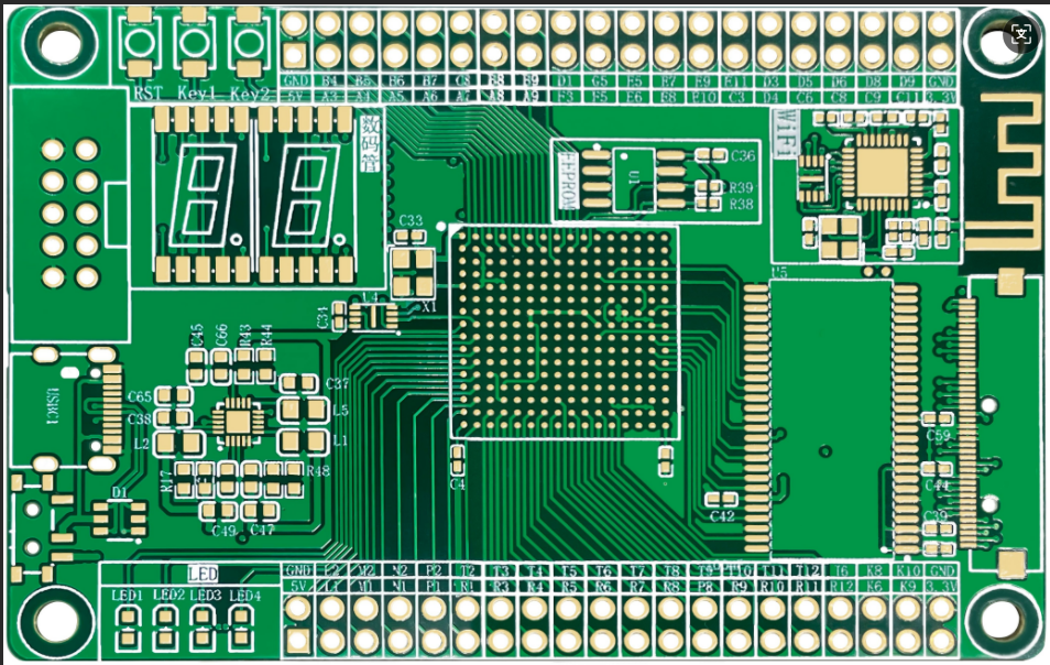
A PCB (Printed Circuit Board) is the foundational building block of almost all modern electronic devices. It's a physical platform that mechanically supports and electrically connects electronic components using conductive tracks, pads, and other features etched from copper sheets laminated onto a non-conductive substrate.
Think of it as the nervous system or the skeleton and roads of an electronic product, providing the structure and pathways for signals and power to travel.

The PCB Manufacturing Process: A Step-by-Step Visual Journey
The process of transforming a design into a physical board is complex and involves many precise steps. Here is a simplified overview:
Step 1: Design and Output
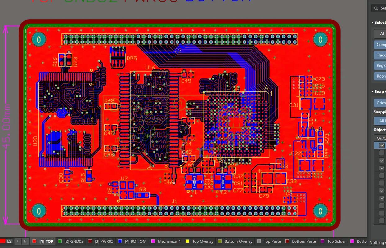
The process starts with a digital blueprint. Engineers use CAD (Computer-Aided Design) software to design the circuit layout. The manufacturer then checks the design for errors before generating output files, typically in Gerber format, which acts as a universal language for PCB fabrication.
 Image: A PCB layout being designed in specialized CAD software.
Step 2: Printing the Inner Layers
The design is printed onto a film, which is then used to transfer the circuit pattern onto the board's core. The core is a laminate board coated with a layer of copper. A photosensitive film called photoresist is applied. Under UV light, the transparent parts of the film harden the photoresist, "printing" the circuit pattern onto the copper.
Step 3: Etching the Copper
The board is then developed, washing away the unhardened photoresist. The board goes through an etching process, where a chemical solution removes the unwanted, exposed copper, leaving only the copper traces protected by the hardened resist.
Step 4: Layer Alignment and Lamination
Modern PCBs are often multi-layered. The inner layers (after being etched) are stacked together with layers of prepreg (a pre-impregnated bonding material) and outer copper foil sheets. This "sandwich" is placed in a laminating press where heat and pressure melt the prepreg, fusing all the layers into a single, solid board.
Step 5: Drilling
Precise holes are drilled through the board using automated drills. These holes will be used for:
Through-hole components: Where component leads are inserted.
Vias: To create electrical connections between different layers of the board.
Step 6: Plating and Copper Deposition
The entire board, including the walls of the newly drilled holes, undergoes a plating process. A thin layer of copper is chemically deposited, which electrically connects the different layers through the vias.
Step 7: Outer Layer Imaging and Etching
Similar to Step 2, the outer layers are coated with photoresist and imaged with the outer layer pattern. The board is then etched again to remove the unwanted outer copper foil, defining the outer circuit traces.
Step 8: Solder Mask Application
The iconic green (or any other color) coating you see on a PCB is the solder mask. It is applied over the entire board and then cured with UV light through a mask that leaves only the solder pads exposed. This layer insulates the copper traces and prevents solder bridges during assembly.
Step 9: Surface Finish
To protect the exposed copper pads from oxidation and to ensure good solderability, a surface finish is applied. Common finishes include:
HASL (Hot Air Solder Leveling): A common, cost-effective finish.
ENIG (Electroless Nickel Immersion Gold): Provides a flat, gold-plated surface, ideal for fine-pitch components.
Step 10: Silkscreen Printing
The final step is printing the silkscreen. This is the white (or other color) lettering on the board that shows component designators, logos, test points, and other helpful information for assembly and debugging.
Step 11: Electrical Test and Final Routing
An automated electrical test verifies the connectivity of the board and checks for any short or open circuits. Finally, the individual boards are routed or scored out of the larger production panel.
Conclusion: From a Blank Slate to a Complex Circuit
The PCB manufacturing process is a marvel of modern engineering, transforming simple raw materials into a highly complex and precise electrical pathway. This bare board, once assembled with components (becoming a PCBA), forms the core of every electronic device we rely on daily.
All images are for illustrative purposes and are sourced from reputable manufacturing and technical websites.

We provide a full range of one-stop electronic components supply chain and manufacturing solutions for customers from all over the world.
Tell: +86-134 8018 3028(Same as Wechat)
Web: www.icslove.com
Skype: jorvih
Add: NO402,4F Xinhongtian building, Fuhai Industrial Zone ,Bao'an district, Shenzhen China.

